MY-CAM003M MIPI Camera Module
The MY-CAM003M MIPI Camera Module is released by MYIR especially
for working on MYIR's development boards. It is connected with the board through a MIPI-CSI interface (24-pin FPC connector) and supports resolution up to 2592 by
1944 pixels. It is using OV5640 image sensor which is a 5 MegaPixel CMOS camera. The module is measuring only 59mm by 33mm with small form
factor, low power consumption, high performance which can be used in various
products.
 
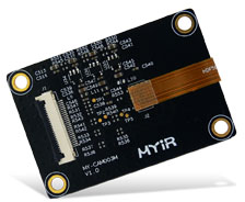
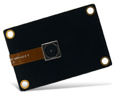
MY-CAM003M MIPI Camera Module (top-view and bottom-view)
USD25 

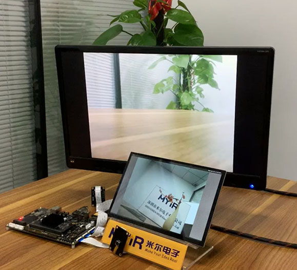
Dual MY-CAM003M Camera Modules working on MYD-JX8MX Development Board
Features
|
Item
|
Paramenters
|
|
Active Array Size
|
2592 x 1944
|
|
Power Supply
|
Core
|
1.5VDC ± 5% (with embedded 1.5V
regulator)
|
|
Analog
|
2.6 ~ 3.0VDC
|
|
I/O
|
1.8V to 2.8V
|
|
Power Requirements
|
Active
|
140 mA
|
|
Standby
|
20 μA
|
|
Temperature Range
|
Operation
|
-30℃ to 70℃ junction
temperature
|
|
Stable Image
|
0℃ to 50℃ junction
temperature
|
|
Output Formats
|
8-/10-bit RGB RAW data
|
|
Lens size
|
1/4″
|
|
Lens chief ray angle
|
24°
|
|
Input clock frequency
|
6~27 MHz
|
|
Max S/N Ratio
|
36 dB (maximum)
|
|
Dynamic Range
|
68 dB @ 8x gain
|
|
Maximum Image Transfer Rate
|
QSXGA (2592x1944)
|
15 fps
|
|
1080P
|
30 FPS
|
|
1280x960
|
45 fps
|
|
720p
|
60 fps
|
|
VGA (640x480)
|
90 fps
|
|
QVGA (320x240)
|
120 fps
|
|
Sensitivity
|
600 mV/Lux-sec
|
|
Shutter
|
Solling shutter / frame exposure
|
|
Maximum Exposure Interval
|
1964 x tROW
|
|
Pixel Size
|
1.4 μm x 1.4 μm
|
|
Dark Current
|
8 mV/s at 60℃ junction temperature
|
|
Image Area
|
3673.6μm x 2738.4μm
|
|
Package Dimensions
|
5985μm x 5835μm
|
Signals
Routed to MIPI-CSI Camera interface (24-pin FPC connector)
|
Pin
|
Signal
|
Description
|
|
1
|
AGND
|
Ground
|
|
2
|
AVDD
|
Power 2V8
|
|
3
|
AF-GND
|
Ground
|
|
4
|
AF-VDD
|
Power 2V8
|
|
5
|
STROBE
|
NC
|
|
6
|
DVDD
|
Power 1V5
|
|
7
|
DGND
|
Ground
|
|
8
|
SCL
|
SCCB data
|
|
9
|
SDA
|
SCCB input clock
|
|
10
|
RES
|
Reset(active low with internal pull up
register)
|
|
11
|
DGND
|
Ground
|
|
12
|
XCLK
|
System input clock
|
|
13
|
DGND
|
Ground
|
|
14
|
MDP1
|
MIPI TX second data lane positive
output
|
|
15
|
MDN1
|
MIPI TX second data lane negative
output
|
|
16
|
DGND
|
Ground
|
|
17
|
MCP
|
MIPI TX clock data lane positive
output
|
|
18
|
MCN
|
MIPI TX clock data lane negative
output
|
|
19
|
DGND
|
Ground
|
|
20
|
MDPO
|
MIPI TX first data lane positive
output
|
|
21
|
MDN0
|
MIPI TX first data lane negative
output
|
|
22
|
DGND
|
Ground
|
|
23
|
PWDN
|
Power down(active hige with internal pull down
register)
|
|
24
|
DOVDD
|
Power 1V8
|
|