Hardware Specification
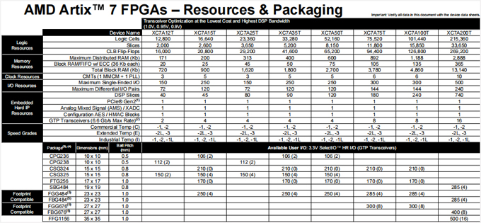
The AMD/Xilinx Artix®-7 family of FPGAs has redefined cost-sensitive solutions by cutting power consumption in half from the previous generation while providing best-in-class transceivers and signal processing capabilities for high bandwidth applications. Built on the 28nm HPL process, these devices deliver best in class performance-per-watt. Together with the MicroBlaze(TM) soft processor, Artix-7 FPGAs are ideal for products like portable medical equipment, military radios, and compact wireless infrastructure. Artix-7 FPGAs meet the needs of size, weight, power, and cost (SWaP-C) sensitive markets like avionics and communications.
The MYC-J7A100T uses the XC7A100T-2FGG484I device, offering an extensive range of features including up to 101,440 logic cells, 4,860 Kb of Block RAM, 240 DSP slices, 929 GMAC/s, 8 GTP transceivers capable of reaching speeds up to 6.6Gb/s, x4 Gen2 PCIe interface, and a total of 285 I/O pins, all contained within the FGG484 package.

1. Supports PCI Express Base 2.1 specification at Gen1 and Gen2 data rates.
2. Represents the maximum number of transceivers available. Note that the majority of devices are available without transceivers. See the Package section of this table for details.
3. Leaded package option available for all packages. See DS180, 7 Series FPGAs Overview for package details.
4. Device migration is available within the Artix 7 family for like packages but is not supported between other 7 series families.
5. Devices in FGG484 and FBG484 are footprint compatible.
6. Devices in FGG676 and FBG676 are footprint compatible.
AMD Artix-7 FPGAs - Resources & Packaging
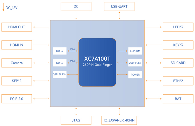
MYC-J7A100T Function Block Diagram

MYD-J7A100T Development Board Function Block Diagram

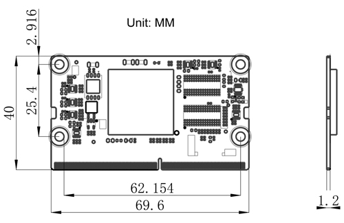
Dimensions of MYC-J7A100T

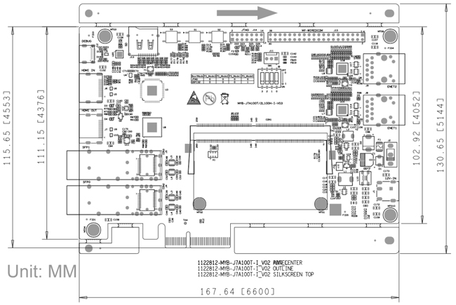
Dimensions of MYD-J7A100T
|