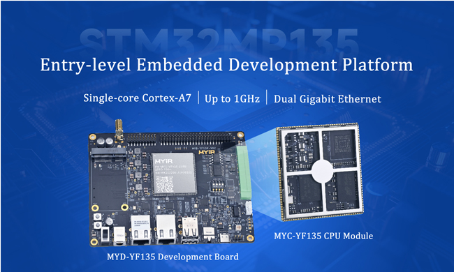
This article will take MYIR’s MYD-YF13X and STM32MP135F-DK as examples, and continue to explain how to use STM32CubeMX combined with the developer package to implement the booting of the minimal system.
Following "Bring up the STM32MP135x - ST Training Course based on MYD-YF13X (I)"
4. USB Boot
USB boot is used for burning image to external flash, e.g. NAND, SD card, etc. The burning image from PC to external flash is completed by U-Boot combined with STM32Cube Programmer. Configuring and compiling U-Boot is a precondition for burning.
According to the STM32 MPU boot sequence:
TF-A->OP-TEE->U-BOOT->Linux Kernel
Loading U-Boot into the DDR depends on TF-A and OP-TEE, sothe configuration and compilation of TF-A, OP-TEE and U-Boot need to be completed in the USB boot phase.
4.1 USB Boot: TFA Configuration and Compilation
During the USB booting stage, the TFA needs to be configured with the following peripherals: Debug serial port UART, Clock RCC, Power Supply and DDR.
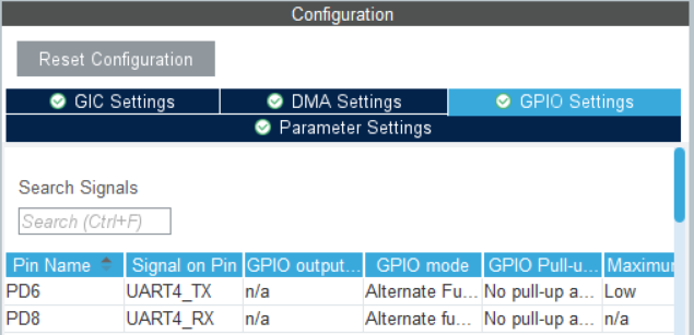
4.1.1 Debugging Serial Port UART
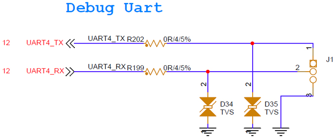
1. Review the schematic and find the debug serial port:
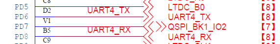
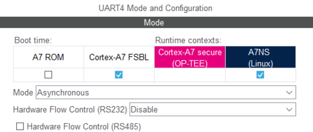
2. Enable UART4, configure the pins and the clock:
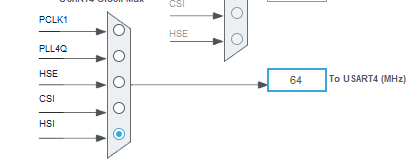
Note: The clock for USART4 is using HSI, one reason is to refer to the clock tree configuration of STM32MP135F-DK, and the other reason is to consider the application of serial port wake-up in low-power working mode. Excluding these two points, other clock sources can also be used.
3. Click "Generate code", and add the user code for the serial port configuration of the TFA stage.
Open the generated STM32CubeMX project, open the TF-A device tree (stm32mp135d-myir_bring_up-mx.dts), and add the nodes "choosen" and "aliases" at the "USER CODE BEGIN root".
/* USER CODE BEGIN root */
aliases {
serial0 = &uart4;
};
chosen {
stdout-path = "serial0:115200n8";
};
/* USER CODE END root */
4. (Optional) Compile the TFA USB image and deploy to the board.
Compile:
PC $> cd
PC $> source
PC $> make -f ../Makefile.sdk TF_A_CONFIG=usb TF_A_DEVICETREE=stm32mp135d-myir_bring_up-mx stm32
Deploy (please make sure the board is powered up, the serial cable and the USB cable are correctly connected before deploying):
PC $> STM32_Programmer_CLI -c port=usb1 -d ../deploy/tf-a-stm32mp135d-myir_bring_up-mx-usb.stm32 0x1 -s 0x1
Serial port printing:
NOTICE: CPU: STM32MP135F Rev.?
NOTICE: Model: STMicroelectronics custom STM32CubeMX board - openstlinux-5.15-yocto-kirkstone-mp1-v22.11.23
ERROR: nvmem node board_id not found
WARNING: VDD unknown
INFO: Reset reason (0x35):
INFO: Power-on Reset (rst_por)
INFO: FCONF: Reading TB_FW firmware configuration file from: 0x2ffe0000
INFO: FCONF: Reading firmware configuration information for: stm32mp_io
INFO: Using USB
INFO: Instance 2
INFO: Boot used partition fsbl1
NOTICE: BL2: v2.6-stm32mp1-r2.0(debug):v2.6-stm32mp-r2-4-g2dedc1cf0-dirty(2dedc1cf)
NOTICE: BL2: Built : 02:45:42, Jun 6 2023
INFO: BL2: Doing platform setup
ERROR: Invalid DDR init: error -22
PANIC at PC : 0x2ffe7739
Exception mode=0x00000016 at: 0x2ffe7739
5. Troubleshooting
If the serial port prints as follows in the previous step or does not print anything:
PANIC at PC : 0x2ffe7739
Exception mode=0x00000016 at: 0x2ffe7739
Then please confirm:
-
Whether the User code has been added to the correct location.
-
Whether the Debug serial port is UART4 and make sure the PIN is configured correctly.
-
Check the hardware connection.
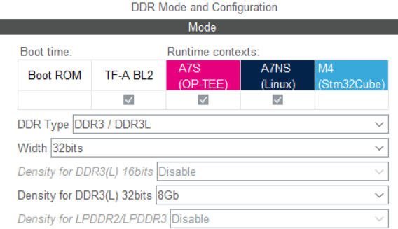
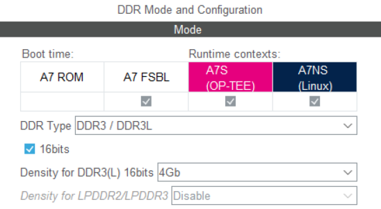
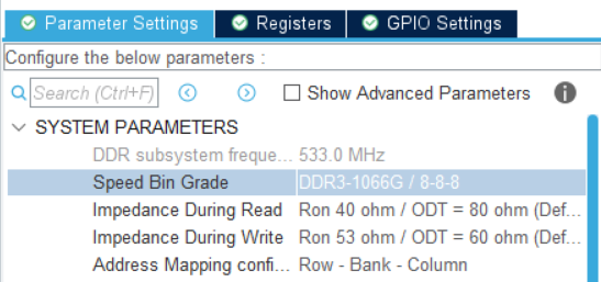
4.1.2 DDR
The following points need to be noted for the DDR configuration:
-
SDRAMS size
-
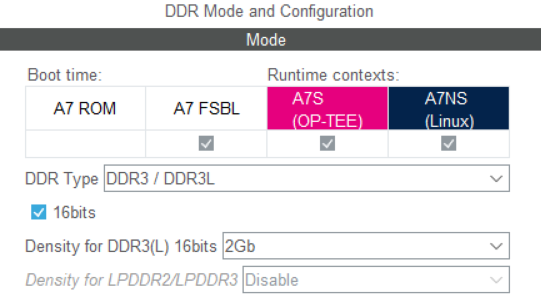
One/two pieces (16/32 bits), STM32MP13x DDR is 16bits, so the configurations are all using 1 piece of SDRAM.
-
DDR types: DDR3/DDR3L/LPDDRx
-
DDR frequency
1. Check the schematic diagram of the DDR design section, confirm the size and frequency and other parameters, and complete the design of the DDR part.
Below are some examples of different DDR designs and their corresponding configurations:
Example 1: STM32MP157C-EV1, two pieces of SDRAM, 32bits, 1GBytes
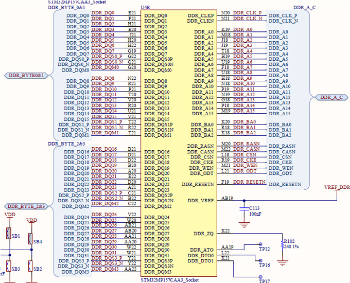
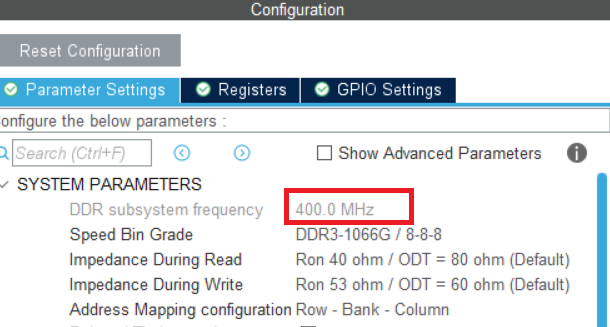
The DDR frequency can be configured in the Configuration interface.
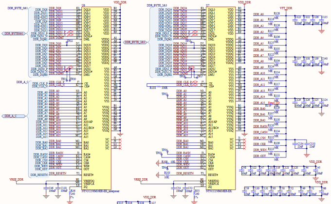
Example 2: STM32MP135F-DK, one piece of SDRAM, 16bits, 512Mbytes.
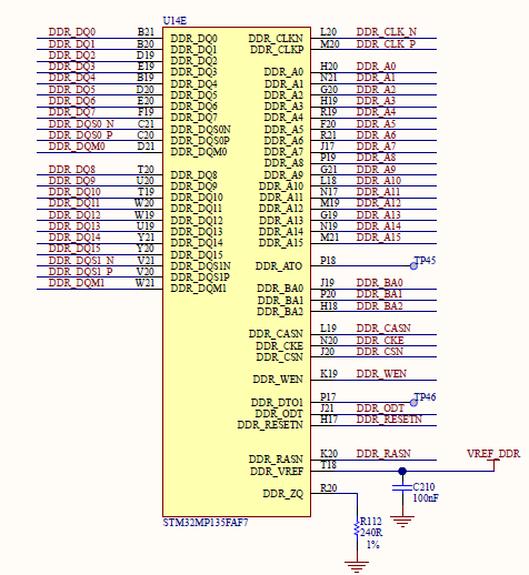
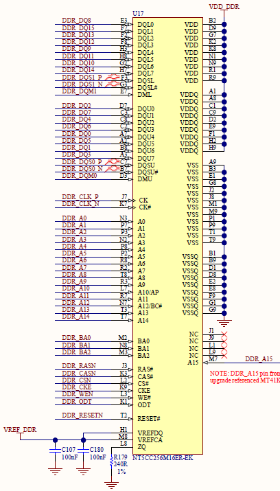
Now let’s take a look at the DDR design part of MYIR’s MYD-YF13X board:
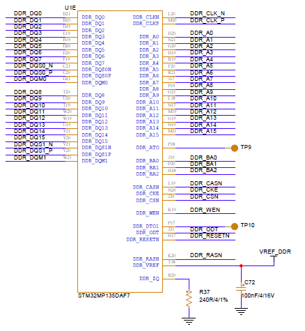
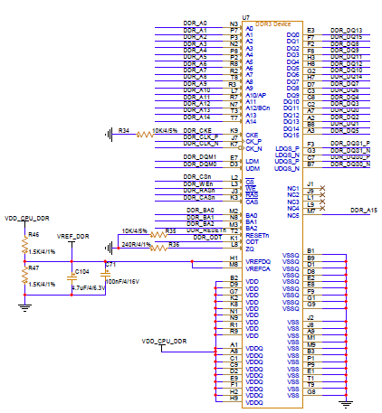
One piece of SDRAM, 16bits, 256Mbytes, STM32CubeMX configured as follows:
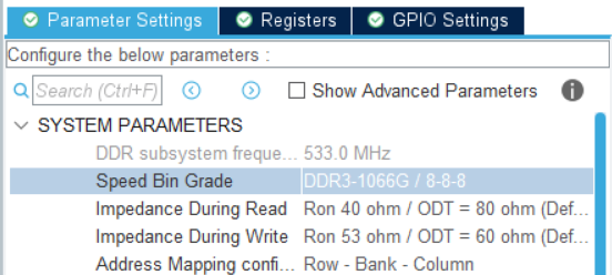
2. DDR Clock Configuration (since the RCC part has not been configured with an external clock, so we first use the internal HSI as the clock source here).
3. Click "Generate code".
4. (Optional) Compile the TFA USB image and deploy to the board.
Compile:
PC $> cd
PC $> source
PC $> make -f ../Makefile.sdk TF_A_CONFIG=usb TF_A_DEVICETREE=stm32mp135d-myir_bring_up-mx stm32
Deploy (please make sure the board is powered up, the serial cable and the USB cable are correctly connected before deploying):
PC $> STM32_Programmer_CLI -c port=usb1 -d ../deploy/tf-a-stm32mp135d-myir_bring_up-mx-usb.stm32 0x1 -s 0x1
Serial port printing:
NOTICE: CPU: STM32MP135D Rev.Y
NOTICE: Model: STMicroelectronics custom STM32CubeMX board - openstlinux-5.15-yocto-kirkstone-mp1-v22.11.23
ERROR: nvmem node board_id not found
WARNING: VDD unknown
INFO: Reset reason (0x30):
INFO: Reset due to a failure of VDD_CORE
INFO: FCONF: Reading TB_FW firmware configuration file from: 0x2ffe0000
INFO: FCONF: Reading firmware configuration information for: stm32mp_io
INFO: Using USB
INFO: Instance 2
INFO: Boot used partition fsbl1
NOTICE: BL2: v2.6-stm32mp1-r2.0(debug):()
NOTICE: BL2: Built : 10:45:30, Jun 28 2023
INFO: BL2: Doing platform setup
INFO: RAM: DDR3-DDR3L 16bits 533000kHz
INFO: Memory size = 0x10000000 (256 MB)
INFO: DFU USB START...
INFO: handle USB : Suspend int
INFO: USB Suspend mode
INFO: handle USB : Reset
INFO: handle USB : Reset
From the above log, we can see that the DDR initialization is successful and the tfa fails at the location where the FW config file is downloaded.
Note: If the customer's power supply design is not a separated power supply, but a PMIC power supply, then the corresponding serial port print should be:
NOTICE: CPU: STM32MP135F Rev.?
NOTICE: Model: STMicroelectronics custom STM32CubeMX board
ERROR: nvmem node board_id not found
WARNING: VDD unknown
INFO: Reset reason (0x35):
INFO: Power-on Reset (rst_por)
INFO: FCONF: Reading TB_FW firmware configuration file from: 0x2ffe0000
INFO: FCONF: Reading firmware configuration information for: stm32mp_io
INFO: Using USB
INFO: Instance 2
INFO: Boot used partition fsbl1
NOTICE: BL2: v2.6-stm32mp1-r2.0(debug):v2.6-stm32mp-r2-5-g38bff70d8-dirty(38bff70d)
NOTICE: BL2: Built : 03:36:12, Jun 6 2023
INFO: BL2: Doing platform setup
INFO: RAM: DDR3-DDR3L 16bits 533000kHz
ERROR: DDR addr bus test: can't access memory @ 0xc0000004
PANIC at PC : 0x2ffe5db1
Exception mode=0x00000016 at: 0x2ffe5db1
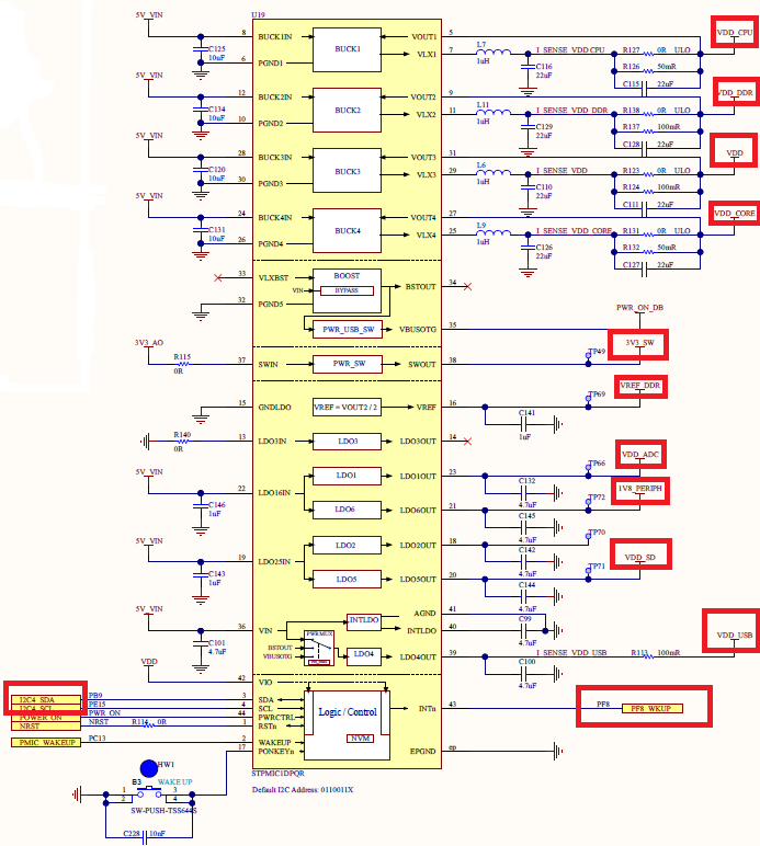
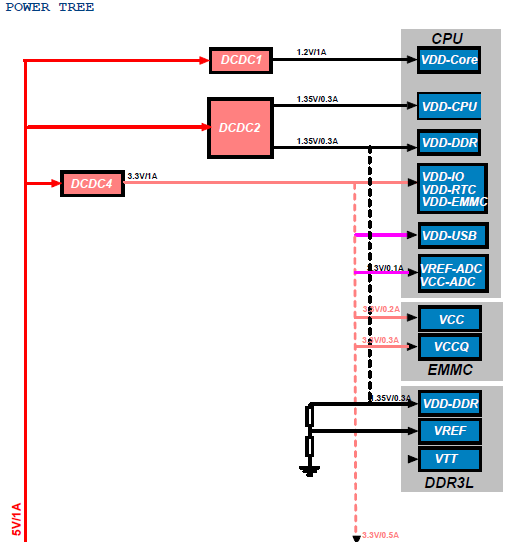
From the perspective of hardware design, the hardware difference involved in the current software configuration is mainly the power supply part. If adopting the separated power supply, once the board is powered up, each DC-DC has an output, without software control, that is, as long as the board is powered up, the DDR power supply already exists; if adopting the PMIC, we take the STM32MP135F-DK board as an example to look at the design of the DDR power supply part:
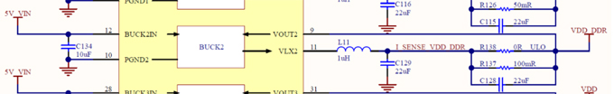
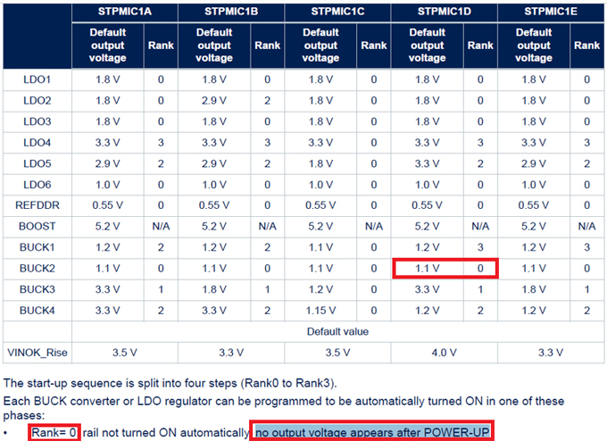
From the schematic diagram, it can be seen that BUCK2 of PMIC is used to supply power to DDR. Meanwhile, according to the datasheet of PMIC, the start-up sequence of BUCK2 is Rank0, and Rank0 has no output by default after power-on, which requires software driver. So if the customer uses PMIC power supply, then the next step is to configure PWR, I2C and PMIC (see 3.1.3).
5.Troubleshooting
Log:
NOTICE: CPU: STM32MP135D Rev.Y
NOTICE: Model: STMicroelectronics custom STM32CubeMX board
ERROR: nvmem node board_id not found
WARNING: VDD unknown
INFO: Reset reason (0x35):
INFO: Power-on Reset (rst_por)
INFO: FCONF: Reading TB_FW firmware configuration file from: 0x2ffe0000
INFO: FCONF: Reading firmware configuration information for: stm32mp_io
INFO: Using USB
INFO: Instance 2
INFO: Boot used partition fsbl1
NOTICE: BL2: v2.6-stm32mp1-r2.0(debug):v2.6-stm32mp-r2-2-g3e0dafdaf(3e0dafda)
NOTICE: BL2: Built : 05:39:48, Jun 5 2023
INFO: BL2: Doing platform setup
INFO: RAM: DDR3-DDR3L 16bits 533000kHz
ERROR: DDR expected freq 533000 kHz, current is 224000 kHz
PANIC at PC : 0x2ffe588f
Ans: If there is a printout as above, please check the DDR clock configuration, one possibility is that PLL2 is not enabled, which can be confirmed through the "Clock Configuration" of CubeMX: the source of AXI Clock is not switched to PLL2P.
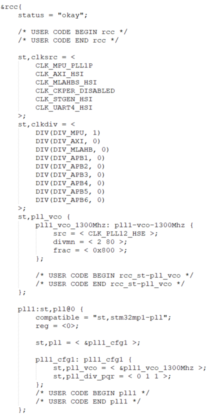
Or you can check whether PLL2 is appeared in the rcc node section of the generated device tree:
4.1.3 PWR
Power supply design is usually two kinds, like the separate power supply used by MYIR and the power management chip STPMIC used by ST demo board, the following will introduce the device tree configuration in two cases respectively.
1. Since the DDR initialization using PMIC power supply failed before, here we take the STM32MP135F-DK as an example to see the configuration of the PMIC and the PWR part:
Let's take a look at the schematic:
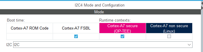
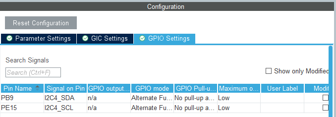
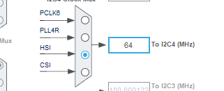
First configure the I2C used to drive the PMIC, the default is I2C4:
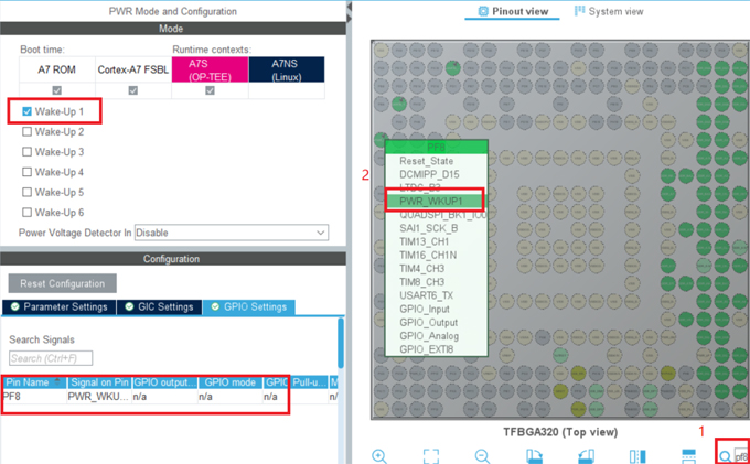
Then configure the wake up pin of PWR:
Click "GENERATE CODE" to generate the device tree, open the tfa device tree to add user code. The configuration of the PMIC part is recommended to copy the configuration of stm32mp135f-dk.dts directly from the tfa source code.Then modify the configuration of the regulator according to the BUCK and LDO outputs of the hardware design:
&i2c4{
pinctrl-names = "default";
pinctrl-0 = <&i2c4_pins_mx>;
status = "okay";
/* USER CODE BEGIN i2c4 */
i2c-scl-rising-time-ns =;
i2c-scl-falling-time-ns =;
clock-frequency =;
pmic:stpmic@33{
compatible = "st,stpmic1";
reg =;
status = "okay";
regulators{
compatible = "st,stpmic1-regulators";
buck1-supply = <&vin>;
…
ldo6-supply = <&vin>;
vref_ddr-supply = <&vin>;
pwr_sw1-supply = <&bst_out>;
pwr_sw2-supply = <&v3v3_ao>;
vddcpu:buck1{
regulator-name = "vddcpu";
regulator-min-microvolt =;
regulator-max-microvolt =;
regulator-always-on;
regulator-over-current-protection;
};
…
v3v3_sw:pwr_sw2{
regulator-name = "v3v3_sw";
regulator-active-discharge =;
regulator-always-on;
};
};
};
/* USER CODE END i2c4 */
};
vin and v3v3_ao of Regulator should also be defined in the device tree. Add the user code should be added to the USER Code BEGINroot node:
/ { /* USER CODE BEGIN root */
vin: vin {
compatible = "regulator-fixed";
regulator-name = "vin";
regulator-min-microvolt =;
regulator-max-microvolt =;
regulator-always-on;
};
v3v3_ao: v3v3_ao {
compatible = "regulator-fixed";
regulator-name = "v3v3_ao";
regulator-min-microvolt =;
regulator-max-microvolt =;
regulator-always-on;
};
/* USER CODE BEGIN root */
Add the PWR node configuration:
&pwr_regulators{
status = "okay";
/* USER CODE BEGIN pwr_regulators */
vdd-supply = <&vdd>;
vdd_3v3_usbfs-supply = <&vdd_usb>;
/* USER CODE END pwr_regulators */
};
Add CPU Supply node configuration:
Compile and deploy to the board and verify that DDR errors are fixed;
After burning, the log prints as follows: DDR errors have been fixed.
NOTICE: CPU: STM32MP135F Rev.?
NOTICE: Model: STMicroelectronics custom STM32CubeMX board
ERROR: nvmem node board_id not found
INFO: PMIC version = 0x21
WARNING: VDD unknown
INFO: Reset reason (0x35):
INFO: Power-on Reset (rst_por)
INFO: FCONF: Reading TB_FW firmware configuration file from: 0x2ffe0000
INFO: FCONF: Reading firmware configuration information for: stm32mp_io
INFO: Using USB
INFO: Instance 2
INFO: Boot used partition fsbl1
NOTICE: BL2: v2.6-stm32mp1-r2.0(debug):v2.6-stm32mp-r2-7-g866f2b026-dirty(866f2b02)
NOTICE: BL2: Built : 12:58:07, Jun 7 2023
INFO: BL2: Doing platform setup
INFO: RAM: DDR3-DDR3L 16bits 533000kHz
INFO: Memory size = 0x20000000 (512 MB)
INFO: DFU USB START...
INFO: handle USB : Suspend int
INFO: USB Suspend mode
INFO: handle USB : Reset
2. Separate Power Supply Design
MYIR’s development board adopts exactly the separated power supply, the schematic diagram is as follows:
When the board is powered on, VDD-Core, VDD-CPU, VDD-DDR, etc. will have power output one after another, no need to be configured by STM32CubeMX or controlled by software, just need to add some user code here:
Add CPU Supply node configuration:
/* USER CODE BEGIN addons */
&cpu0{
cpu-supply = <&vddcpu>;
};
/* USER CODE END addons */
It is also required to define the regulator vdd_cpu that is introduced in the CPU Supply node:
/* USER CODE BEGIN root */
vdd_cpu: vdd_cpu{
compatible = "regulator-fixed";
regulator-name = "vdd_cpu";
regulator-min-microvolt =;
regulator-max-microvolt =;
regulator-always-on;
};
/* USER CODE END root */
4.1.4 RCC
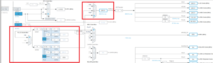
RCC, Reset and clock control. the RCC module is responsible for the control of internal clocks (LSI, HSI and CSI) and external clocks (LSE and HSE). These internal and external clock sources provide clock signals to the hardware module directly or indirectly (via PLLs).
-
PLL1 is used as the clock source for the MPU.
-
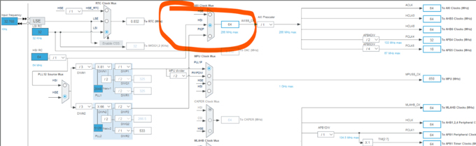
PLL2 provides clocks for AXI-SS (including APB4, APB5 and APB6), DCMIPP and DDR.
-
PLL3 provides clocks for MLAHB, APB1, APB2, APB3, AHB, etc., as well as peripheral clocks.
-
PLL4 provides clocks for various peripherals.
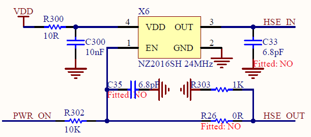
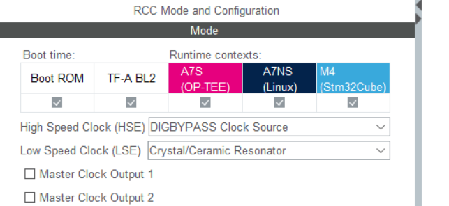
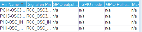
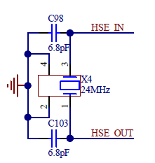
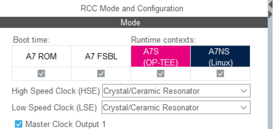
This section describes how to configure to enable the external clocks LSE and LSE. First look at several classic design circuits for the HSE:
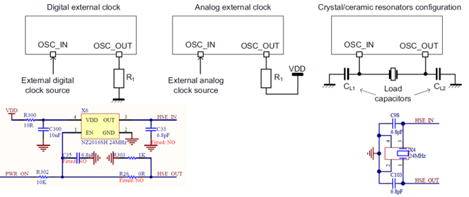
The differences in software configuration between the different hardware design modes are as follows:
Example 1: STM32MP157C-EV1
Example 2: STM32MP135F-DK
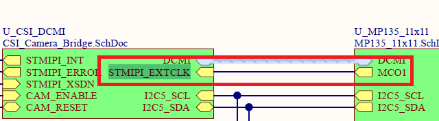
The RCC can provide two output clocks (MCO1, MCO2) which can be used as clock source for external devices.
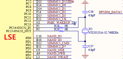
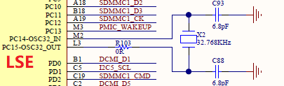
With the two examples shown above, we take a look at MYIR’s design:
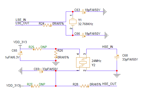
The HSE uses the same passive crystal design as the STM32MP135F-DK, so the STM32CubeMX is configured as follows:
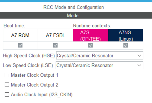
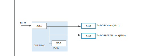
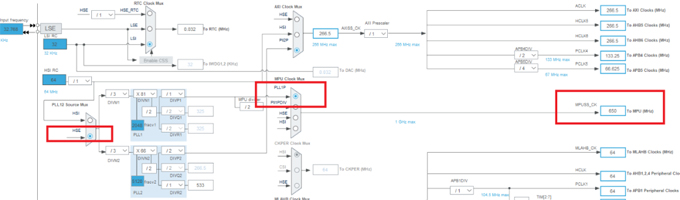
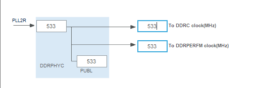
Switch to "Clock Configuration" interface. Set the clock source of PLL1 and PLL2 to HSE, and make sure the clock frequency of DDR is set to 533Mhz, and the main frequency of CPU is configured to 650Mhz:
Click "Generate code", compile TF-A and deploy it to the board, the serial log output should be the same as the previous step.
If the print out log is different from the previous step after RCC is configured, the serial port will print the following panic:
PANIC at PC : 0x2ffecb43
Exception mode=0x00000016 at: 0x2ffecb43
Please check the configuration of HSE in STM32CubeMX, and if you confirm that there is no problem with the configuration, please check the hardware connection.
|

